SIB62 – HF-Circuits
Metrology for new electrical measurement quantities in high frequency circuits
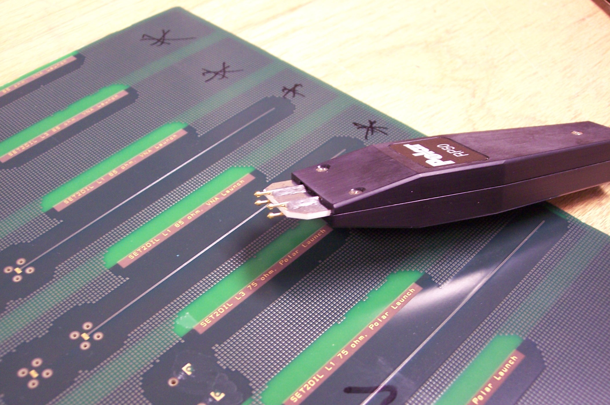
WP3 Traceable Differential S-parameter Measurements of Planar Circuits to Test Signal Integrity
Work Package Leader: NPL
Other participants: CMI, LNE, PTB, R&S, CTU, FBH
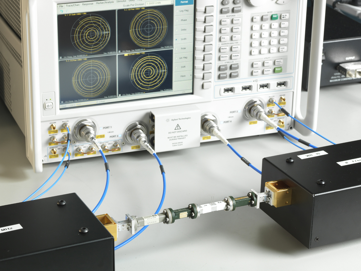
This Work Package has put in place traceable measurement facilities for differential S-parameter measurements of devices with balanced (i.e. two-conductor) input/output ports.
At the time of the project, the state-of-the-art relating to differential S-parameter measurements was that all the major test equipment manufacturers of RF and microwave Vector Network Analysers (VNAs) offered the capability to measure differential S-parameters. This was achieved using either 'superposition' or 'true' differential stimuli using four-port VNAs. Some VNAs offer both these methods of measurement. However, at the time of the project, there was no traceability available for either of these measurement methods. This had a detrimental impact on the ability to demonstrate the accuracy and reliability of these measurements. This, in turn, impacted the ability to provide quantitative Signal Integrity indications for digital signal measurements on planar circuit layouts, such as Printed Circuit Boards (PCBs).