Measurement and control of single-photon microwave radiation on a chip
WP4: Technology development
Workpackage leader: Dr Emanuele Enrico, INRIM
Other participants: MIKES, PTB, NPL, Aalto, RHUL, LanU
The aim of this workpackage is to design the layout, estimate and choose the parameters and establish fabrication processes for the devices necessaries for WP1, WP2, and WP3. An optimised measurement infrastructure will also be developed within this workpackage. Development of microwave sources and detectors based on various nanoelectronic circuits, such as single-electron transistors, qubits or quantum dots requires the use of advanced nanofabrication methods and low-temperature ultra-low-noise measurements involving microwave techniques.
Below is a brief description justifying the use of these techniques. Nanoelectronic devices consist of ultrasmall tunnel junctions and islands, with a typical size well below 100 nm, which is beyond the reach of conventional photolithography. In addition to the small sizes, these devices require formation of a high quality tunnel barrier, which is usually done in situ by introducing oxygen gas into an evaporation chamber. Thus, for the fabrication of these devices, a combination of electron-beam lithography, dry etching and angle deposition is commonly used. Focused ion beam will also be utilised for certain tasks. Besides the small feature size, which is a must for this type of device, often nanoelectronic circuit components on a chip need to be precisely positioned. Examples of such circuits include (i) a single Josephson junction, a qubit or a quantum dot coupled to a planar on-chip resonator; (ii) a narrow normal-metal thin-film piece connected to the central line of a superconducting resonator and playing the role of a matching load; (iii) an integrated circuit comprising a photon source and a photon detector mediated, for instance, by an on-chip waveguide.
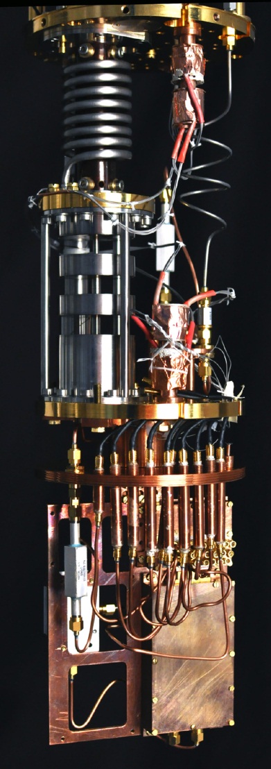
These are exactly the circuits that will be developed within this project. The typical energy of microwave photons is very low. For example, a single photon having a frequency of 15 GHz will have an energy of 10 ^-23 J, which corresponds to the temperature of thermal fluctuations of 1 K, only. Therefore, to be operational, the microwave sources and detectors should have a cold environment, ideally with T << 1 K. Such an environment can be provided by a dilution refrigerator capable of reaching working temperatures of a few mK. Even if such a low temperature is achieved, special care must be taken to protect the source and detector from the black body radiation coming from the warmer parts of the cryostat. This includes filtering of dc and microwave lines coming from room temperature to the mixing chamber stage as well as installing multiple shields around the sample holder. These issues affect the performance of sources and detectors as well as other nanoelectronic components, and a measurement system for characterising and minimising these effects will be developed in this WP.
The research within this EURAMET joint research project receives funding from the European Community's Seventh Framework Programme, ERA-NET Plus, under Grant Agreement No. 217257.
For more information, please contact the project coordinator, Dr Antti Manninen from MIKES