Traceable characterisation of nanostructured devices
The micro and nano electronic world is experiencing a revolution in tackling the new challenges in terms of miniaturisation, power consumption, power density and processing speed. Novel inorganic semiconductor materials (Ge, InGaAs, GaN, SiC, etc.) and new 3D-architectures (Multiple Gates FETs, Nanowire T-FETs, etc.) with feature sizes < 30 nm are replacing traditional silicon devices. There is now a critical need for metrology to give traceable and quantitative chemical composition measurement of new materials in complex spatial arrangements with buried interfaces and with nm depth resolution.
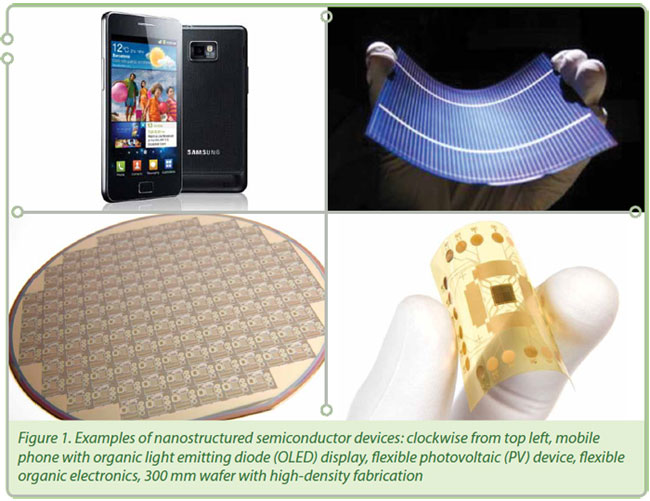
Concurrent with these developments is the emergence of electronics based on organic semiconductors, made of single molecules in highly ordered assemblies and polymeric semiconductors in thin films. This is an important new knowledge-based, high innovation and high value (multibillion €) sector for the EU.
Unfortunately, the techniques developed for the inorganic semiconductor industry do not directly apply and there is an urgent need for methods to give 3D nanoscale chemical and electrical imaging. The current state of the art, 3D SIMS with C60 sputtering fails completely for organic electronic materials and there are no existing methods for 3D nanoscale electrical measurements.
The challenges here are for metrology at the nanoscale and it is clear that no single technique
can provide all the answers required by industry. Whilst a single technique may offer repeatable
high precision results, the accuracy (closeness to a true value) of all techniques is limited.
This causes major difficulties in manufacturing and research and development since a complete
nanoscale picture cannot be reliably assembled. The solution is traceability of these nanoscale
measurements
