The Project
Download Final Publishable Summary
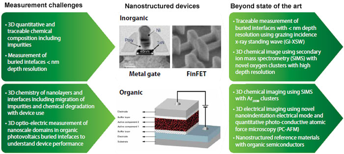
The aim of the proposed JRP is to develop traceable measurement and characterisation of physical and chemical properties of the next generation of integrated nano structured devices with sub 30 nm dimensions using novel 3D architectures.
- Improvement of non-destructive methods for the characterisation of nanolayers and buried interfaces, by chemical depth-profiling of nanolayers (up to 200 nm) with trace level sensitivity.
- Development of essential metrology to enable 3D nanoscale chemical imaging of organic electronic materials using new massive argon cluster sputtering combined with secondary ion mass spectrometry (SIMS). This will be done by 3D chemical characterisation of nanolayers and interfaces with depth resolutions of better than 10 nm at depths of up to 400 nm and spatial resolution better than 100 nm.
- Development of a novel method for 3D nano-electrical characterisation of organic semiconductor nanostructures and nanostructured self-assembled reference materials (with resolution better than 30 nm) for the metrological studies of the techniques.
Consortium
The JRP-Consortium has a large number of stakeholders, many of whom have indicated an interst in active collaboration with the JRP-Consortium. These stakeholders will be informed of the JRP progress, and who it is hoped may become early adopters of the JRP outputs
The integration of one unfunded JRP-Partner and two REG-Researchers at world-leading Home Organisations, along with the use of existing stakeholder networks will enable a two-way information route to over a 100 EU enterprises involved in inorganic and organic electronics.
