Work Packages
Please click a Workpackage for more information
Workpackage 1: Traceable chemical and depth characterisation of inorganic nanolayers and buried interfaces (PTB)
The objective of this workpackage is to improve non-destructive methods that are used for the characterisation of nanolayers and buried interfaces, i.e. chemical depth-profiling of nanolayers with trace level sensitivity and high information at depths up to 200 nm.
The current metrological requirements in the development and fabrication of novel nanostructured device materials are increased reliability, reduced uncertainties and improved traceability. The tasks of this workpackage address several developments beyond the state-of-the-art in order to fulfil the present metrological development as well as fabrication requirements of novel device materials.
Workpackage 2: 3D Nanoscale chemical imaging of organic electronic materials (NPL)
The objective of this workpackage is to improve non-destructive methods that are used for the characterisation of nanolayers and buried interfaces, i.e. chemical depth-profiling of nanolayers with trace level sensitivity and high information at depths up to 200 nm.
The current metrological requirements in the development and fabrication of novel nanostructured device materials are increased reliability, reduced uncertainties and improved traceability. The tasks of this workpackage address several developments beyond the state-of-the-art in order to fulfil the present metrological development as well as fabrication requirements of novel device materials.
Workpackage 3: 3D nano-electrical and optical characterisation of organic semiconductor nanostructures (INRIM)
This WP aims to develop methods for reliable measurement of 3D morphology by
- Combining Transmission electron microscopy (TEM) tomography and Electron Energy Loss Spectrometry (EELS).
- Advanced scanning probe methods that combine topographical data with electrical or opto electrical characterisation to enable both surface and subsurface discrimination. This includes the development of AFM based nano-indentation combined with an electrical mode.
The WP will combine experimental measurements with theoretical modelling to establish reliable uncertainty budgets and measurement procedures. The experimental measurements will be based on well-characterised samples, based on cutting-edge commercially relevant materials (e.g. working organic nanostructured solar cells)
Workpackage 4: Creating Impact (PTB)
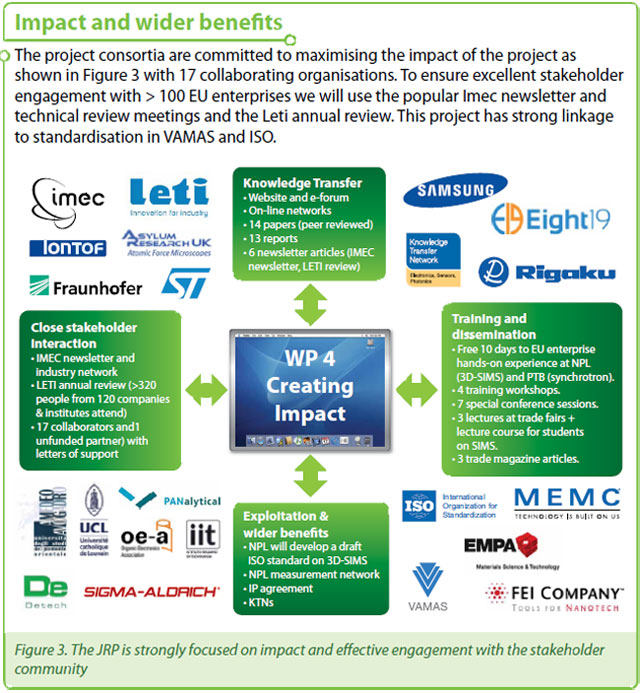
The activities in this workpackage aim at increasing knowledge to support innovation and competitiveness of the European inorganic and organic nanoelectronic competences ranging from the industrial, academic to the metrology sector.
Workpackage 5: Management and Coordination (NPL)
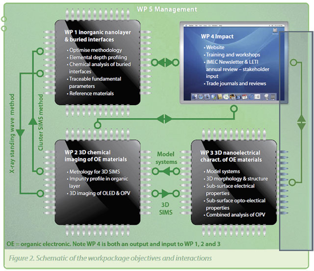
This WP outlines the project management that will be put in place to deliver the JRP.
The JRP-coordinator (NPL), leads this task, and has a proven track record for delivering multi-national collaborative projects. NPL will use an experienced and dedicated project leader to coordinate the work, enabling the scientists to focus and carry out the technical research
- Workpackage (WP) leaders: will be allocated for each WP: they liaise with all WP participants to ensure work to plan and on schedule, so that the deliverables are achieved on time. Any issues that cannot be resolved will be discussed at JRP-meetings.
- REG management: REG-Researchers directly report to the WP leader and JRP-Coordinator, who will escalate issues as required.
